
The 11 Stages of the Electronics Manufacturing Process
- Key Takeaways
- Stage 1: Design Review and DFM
- Stage 2: Prototyping and Validation Builds
- Stage 3: Component Sourcing, Procurement and Kitting
- Stage 4: Bare PCB Fabrication
- Stage 5: SMT Assembly
- Stage 6: Through-Hole and Selective Soldering
- Stage 7: Secondary Processes
- Stage 8: Enclosure Fabrication and Finishing
- Stage 9: Box Build and Final Assembly
- Stage 10: Test and Inspection
- Stage 11: Compliance, Packaging and Logistics
- Which Standard Apply at Which Stage
- FAQ
The electronics manufacturing process runs through eleven stages: design and DFM review, prototyping and validation builds, component sourcing and kitting, bare PCB fabrication, SMT assembly, through-hole and selective soldering, secondary processes such as depanelization and conformal coating, enclosure fabrication, box build and final assembly, test and inspection, then compliance documentation and shipping.
It doesn't end when the boards have been assembled. Launch delays are usually caused by what comes after that, and the enclosure is the usual culprit.
No single company handles all eleven. A complete build involves several manufacturers and suppliers, and your contract manufacturer almost certainly buys bare boards from a specialist fabricator rather than making them. As the client, your job is to make the product and design decisions and to coordinate every vendor involved.
Main Takeaways
Most contract manufacturers buy bare boards instead of building them.
The schedule for a full assembly is based largely on lead times for each individual component. As of March 2026, lead times for some semiconductors hit 40 weeks.
Most of the stages in the manufacturing process are governed by IPC standards and should adhere to its specifications and guidance.
Surface finishes for bare PCBs have different shelf lives, so clients should make sure to select a finish that won't wear out before the board can be finished.
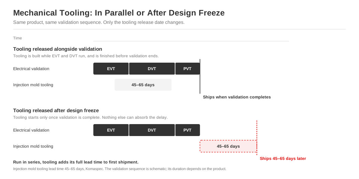
Mechanical tooling has to run in parallel with electrical validation. Injection molds take 45 to 65 days, and run in series that time is added to your launch date.
"Build to IPC standard" is not a specification. Name the standard, the revision, and the class in the contract.
Table of Contents
- Main Takeaways
- Stage 1: Design Review and DFM
- Stage 2: Prototyping and Validation Builds
- Stage 3: Sourcing, Procuring and Kitting Components
- Stage 4: Bare PCB Fabrication
- Stage 5: SMT Assembly
- Stage 6: Through-hole and Selective Soldering
- Stage 7: Secondary Processes
- Stage 8: Enclosure Fabrication and Finishing
- Stage 9: Box Build and Final Assembly
- Stage 10: Testing and Inspection
- Stage 11: Compliance, Packaging and Logistics
- Which Standards Apply at Which Stage
- Frequently Asked Questions
Stage 1: Design Review and DFM
Design for manufacturability (DFM) is the step where a manufacturer evaluates your design to ensure that it is practical and feasible. Based on your drawings and bill of materials (BOM), they will tell you whether making the product will be too expensive, drag out production time, or is simply unbuildable. For an electronic product, they might flag specific issues like component footprints that don't match the parts you specified, test points the fixtures can't actually reach, or parts cramped too close together.
This review stage is a massive cost saver. If the manufacturer catches a problem with a component's footprint in your CAD file, this can be fixed with a quick design revision. But if they only catch it after assembling the first article, fixing it needs a new stencil, a scrap panel, and weeks added to your timeline.
For your DFM review, send your mechanical files and electrical files at the same time. Why? Because some errors happen because of a mismatch between them. If your assembler only has the board designs and the machine shop only has the enclosure drawings, no one can check that the tolerances between the PCB, the standoffs, and the sheet metal stack up properly. It becomes another issue that's only discovered once the product is put together, and fixing it becomes a lengthy and expensive process.
Be mindful of the file types you're sending. While your fabricator can work with plain RS-274X files, they don't have the netlist and stackup data that Gerber X2 and IPC-2581 files contain. Without that information, they'll need to get it from you, which could delay the review.
And make sure your BOM lists actual manufacturer part numbers, not just descriptions of each material. Listing something like "10uF 0805 Ceramic" only raises more questions because that category includes a hundred different parts that can have different temperature coefficients.
Stage 2: Prototyping and Validation Builds
Validating your product's hardware will usually require three tests.
First, the Engineering Validation Test (EVT) builds a small batch of units to verify that the design works at all. Quantities are set by what you need to test, not by a rule of thumb.
Second, the Design Validation Test (DVT) builds a larger batch and puts it through drop, thermal, lifecycle, and certification testing. This is usually the longest of the three, because environmental testing and certification samples gate it.
Finally, the Production Validation Test (PVT) is a pilot run on production tooling with production operators. DVT proves the design; PVT proves the factory can reproduce it. Ask your manufacturer for their own quantities and durations early, because they vary widely by product and by factory.
Stage 3: Sourcing, Procuring and Kitting Components
If you're currently having scheduling problems, it's probably because lead times are getting longer for some components. Passive components have lead times up to 20 weeks right now. And according to Accuris, lead times for some semiconductors hit the 40-week mark in March 2026, a 67% jump in a single month.
Forty weeks is longer than most hardware development programs. So if one of the items on your BOM takes that long to arrive, it can drag down your entire timeline. You can potentially speed things up by selecting approved alternate parts and vendors during DVT. This gives your manufacturer some flexibility with materials, which can help them deal with shortages and hit your target shipping date.
Kitting gets overlooked, but it's important for protecting the integrity of components. Moisture-sensitive devices have a floor life set by the IPC/JEDEC J-STD-020 and J-STD-033 standards. If you're kitting an MSL 3 part, it has a limit of 168 hours of exposure at 30°C and 60% RH before it has to be baked. With MSL 4, it's 72 hours. And MSL 5a only gives you 24 hours. Exceed those limits and the part can popcorn, meaning the trapped moisture turns to steam and cracks the package from the inside. If you build with those components, the product might look fine on the outside but then fail once it's put to use.
Stage 4: Bare PCB Fabrication
The bare board is a separate manufacturing process that needs to be handled by a specialist. Those specialists first image and etch copper-clad laminate to build the board's inner layers, then press those layers together with prepreg under heat and pressure. Then they drill and chemically plate holes, etch the outer layers, and add the solder mask and silkscreen. Finally, they'll apply the surface finish to protect the exposed copper and check every net (using a flying probe or bed-of-nails test) before shipping out the panels.
Most contract manufacturers don't do any of that. They buy the finished panel. That means the fabrication specification is yours to write, and there are two things to watch for when you do.
The performance class. IPC-6012 provides qualification and performance requirements for rigid boards across Class 1, 2 and 3. And IPC-A-600 is a visual guide that shows what boards meet the requirements and which ones don't.
Class 3 has the strictest requirements. It sets tighter targets for plated through-hole copper thickness, requires a positive annular ring for every layer, and narrows the acceptance windows on basically every measure. Meeting Class 3 costs more and yields worse, so only specify it if your application genuinely requires it. If it does, say so before fabrication starts. A board built to Class 2 tolerances can't be certified to Class 3 afterwards, even if it happens to measure inside the limits.
The surface finish. Your board's finish determines whether it solders cleanly and how long it can sit before being soldered.
| Finish | Fine pitch / BGA | Shelf life | Notes |
|---|---|---|---|
| HASL | Not suited to fine pitch or BGA | 12 months | Cheapest, uneven surface, fine for through-hole-heavy boards |
| ENIG | Yes | 12 months | Flat pads, the default for BGA work, costs several times OSP, carries black pad risk if plating is poorly controlled |
| OSP | Yes | 6 months | Lowest cost and flat, degrades under multiple reflow cycles, don't bake it |
| Immersion silver | Yes | 6 months | Good high-frequency performance, tarnishes without sulphur-free packaging |
| Immersion tin | Yes | 6 months | Flat, degrades through intermetallic growth |
The shelf life column of this table is based on IPC-1601 storage guidance for boards kept under 70% RH, as per GE Vernova's component storage specification. These are not final numbers - individual vendors will give you different quotes for the same finish depending on the grade and packaging.
The common mistake here is buying the cheapest finish and then holding the boards. If one of your components has a 40-week lead time, that means the bare boards will sit for eight months before assembly even starts. So going with OSP to get a cheaper quote could backfire if it doesn't have the shelf life you need.
Stage 5: SMT Assembly
Surface mount (SMT) assembly is itself a five-step process: solder paste printing with a laser-cut stencil, solder paste inspection (SPI), high-speed pick-and-place, reflow, then automated optical inspection (AOI).
Reflow is where tolerances really matter. SAC305, the standard lead-free alloy, becomes liquid at 217°C, and a typical Pb-free profile per IPC/JEDEC J-STD-020 holds a peak of 240 to 245°C with no more than 90 seconds above liquidus, a ramp-up limit of 3°C per second and ramp-down no faster than 4°C per second. That leaves only about 25°C of headroom between the alloy going liquid and the peak the profile targets. And it has to stay within this range across a board carrying both an 01005 passive and a shielding can with far greater thermal mass.
This is why profiling is done per assembly, not per line. A profile that was validated on your last product doesn't necessarily work for the one that's currently being built.
You could technically skip the SPI, but then you might only uncover problems during the AOI (or even later). It's better to find out that there isn't enough paste, bridging, or offset prints while you're still at the printing stage. It's going to be more expensive if you only uncover these issues once the components are in place. So make sure the electronics manufacturing quotes you're considering show SPI as part of the process.
Stage 6: Through-hole and Selective Soldering
Once the SMT line is through with the board, it goes through this next phase where additional components are added. That includes the connectors that take mechanical load, large electrolytics, transformers, heavy inductors, and anything the customer might plug and unplug countless times.
Selective soldering has mostly displaced wave baths for high-mix work. Which makes sense, because a wave bath drags the entire underside of the assembly through molten solder even if it doesn't need it. That rules it out for boards carrying bottom-side SMT, unless you're willing to pay for pallets and masking.
Selective soldering targets individual joints. That makes it slower per unit, so you might still want to go with a wave bath if you're running high volumes of a single-sided assembly that's heavy on the through-holes. But for everything else, selective soldering is a better bet.
Cable and wire harnesses are built at this stage. They follow the IPC/WHMA-A-620 standard, and how much they'll cost you will depend on the class you specify. That's a topic we've covered separately in our wire harness assembly guide.
Stage 7: Secondary Processes
Once the soldered panel is done, there are still a few more processes left to do. It can be tempting to think of these as "extra steps" but they're responsible for a large share of field failures, so it's worth taking them seriously.
Depanelization. Boards are built in panels and separated at a later stage, using one of three methods. V-scoring cuts a groove about 30% of the board's thickness into each side, and the panel is then snapped or run through a cutting wheel. Routing mills the outline instead. Laser cutting separates the panels without physical contact, and therefore without mechanical stress. The method matters because board flex cracks multilayer ceramic capacitors (MLCCs). A cracked MLCC will pass electrical testing in the factory but fail sooner than it should once it's in service. Make sure to also keep MLCCs well clear of the score lines, and use routing or laser for boards that have BGAs or dense fine-pitch work.
IC programming. Firmware gets loaded into the board. This is either done by the assembler (in-line, using a programmer or bed-of-nails fixture) or after assembly (in-circuit through a JTAG or SWD). You should decide who does the programming early on because in-circuit programming requires an accessible header and a test fixture that can reach it, so this will affect your board's layout. If you push off this decision and need to retrofit the layout, that will cost you a board respin.
Conformal coating. Anything intended for a humid, dusty, or condensing environment has to be coated. IPC-CC-830 qualifies the coating material and IPC-A-610 governs how the applied coating is inspected. Acrylic and polyurethane coatings typically run 25 to 75µm thick, while silicones go from 50 to 210µm.
Stage 8: Enclosure Fabrication and Finishing
The launch date for a typical electro-mechanical product depends on its mechanical parts more than the PCB.
Once the assembler receives all the components, they can build the PCBA in a matter of days. But the enclosure doesn't come together as quickly. It takes around 45 to 65 days to build an injection mold. And once the mold is done, you still need T1 samples, dimensional reports, and steel adjustments before you can make a part that's actually ready to ship.
The timeline is faster if you're using sheet metal for the enclosure, because you can set laser cutting and CNC bending to go without creating any custom tooling. But even then, you'll need process time for the powder coating, silkscreen, and hardware insertion. And if you're making a bent part with tight hole-to-edge tolerances, it will probably take a few rounds before getting first-article approval.
The best way to speed up your schedule is to run your mechanical tooling while the electronic components are undergoing EVT and DVT. If you wait for those steps to be done, you're adding about two months to your product's launch date.
This is also where vertical integration earns its keep. When sheet metal fabrication, plastic injection and electronics assembly sit under one roof, a fit problem between the enclosure and the board is one supplier's problem to solve. Split across three vendors, it becomes a three-way argument about whose drawing was right.
Stage 9: Box Build and Final Assembly

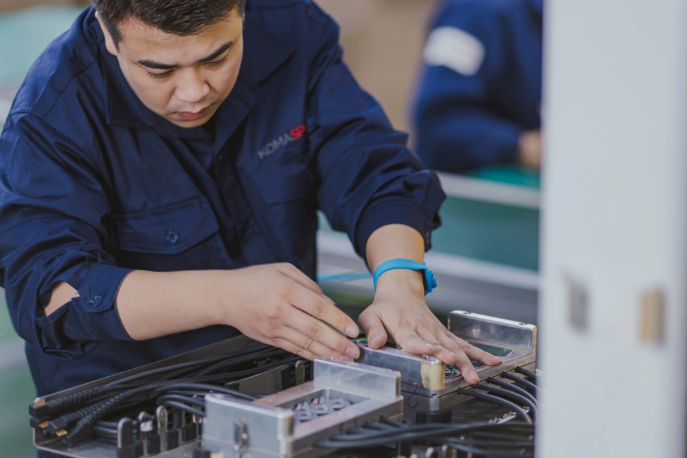
These poka-yoke solutions are more reliable than training personnel to avoid mistakes. An operator told to check connector orientation will get it right almost every time, and almost every time is a field failure rate. A fixture that won't close on a reversed connector removes the judgement call entirely. That difference is why fixtures, rather than work instructions, are what a box build assembly line is actually built around.
Stage 10: Testing and Inspection
There are four types of test, and each covers a different failure mode. They're not interchangeable, so it's best to use more than one type.
| Test | Finds | Doesn't find |
|---|---|---|
| AOI | Placement, polarity, visible solder defects | Hidden joints under BGAs, electrical faults |
| X-ray | Voiding, opens and bridges under BGAs and QFNs | Functional failures |
| ICT (in-circuit) | Wrong, missing, damaged or misplaced components; shorts | System-level behaviour, firmware issues |
| FCT (functional) | Whether the product does its job | Which component caused the failure |
Add burn-in wherever infant mortality matters. The product is run powered at raised temperature for a defined period, which forces early-life failures to happen before shipment rather than after.
Your product's workmanship gets evaluated according to IPC-A-610 (which has been revised to Revision J in July 2024). The exact requirements will depend on whether your product falls under Class 1 (General Electronic Products), Class 2 (Dedicated Service Electronic Products), or Class 3 (High Performance Electronic Products). Specify the class in your contract. "Build to IPC standard" is not a specification, and the gap between Class 2 and Class 3 shows up in inspection coverage, rework rules, and price.
Stage 11: Compliance, Packaging and Logistics
The final stage is about documentation and protection.
Restriction of Hazardous Substances (RoHS) is the baseline for any product destined for the EU. Directive 2011/65/EU caps lead, mercury, hexavalent chromium, PBB, and PBDE to 0.1% by weight, and cadmium at 0.01%. Those limits apply for each material in the product. So even if everything is compliant except for one single connector plating, the unit doesn't pass. Prepare for this by collecting declarations when you're qualifying components, instead of waiting to be asked to produce them once your product lands at the border.
UL, ETL, and CSA safety certifications take longer and require more planning than most companies assume, so get started on these early. We've covered this process separately.
Like the product itself, its packaging should be tested rather than assumed. Put it through drop, vibration, and compression testing in the actual shipping configuration. It is far cheaper to find out that a carton fails a drop test on a bench than after a container has landed.
This is also the stage where paperwork comes into play, including HS codes, country-of-origin documentation, and certificates of conformity. Even though you only need them now, these should all have been settled at Stage One instead of trying to cobble them together at the last minute.
Which Standards Apply at Which Stage
Eight of the eleven stages have a published standard governing them directly, and a quality management system sits under all of them. Name the applicable standard, revision, and class in your contract to avoid arguments over quality.
| Stage | Standard | Covers |
|---|---|---|
| 1 — Design | IPC-2221 | Generic PCB design requirements |
| 4 — Bare board | IPC-6012 / IPC-A-600 | Rigid board performance and visual acceptability |
| 3 — Kitting | J-STD-020 / J-STD-033 | Moisture sensitivity classification and floor life |
| 5, 6 — Soldering | J-STD-001 | Soldered assembly process requirements |
| 5, 6, 10 — Workmanship | IPC-A-610 | Acceptability of electronic assemblies |
| 6 — Harnesses | IPC/WHMA-A-620 | Cable and wire harness assembly |
| 7 — Coating | IPC-CC-830 | Conformal coating qualification |
| 10 — ESD | ANSI/ESD S20.20 | Static control program requirements |
| 11 — Compliance | RoHS 2011/65/EU, REACH | Restricted substances |
| All | ISO 9001, ISO 13485, IATF 16949 | Quality management system, by sector |
Frequently Asked Questions
What are the stages of the electronics manufacturing process?
There are eleven stages, in the following order: design and DFM review, prototyping and validation builds, sourcing and kitting components, bare PCB fabrication, SMT assembly, through-hole and selective soldering, secondary processes, enclosure fabrication, box build, testing and inspection, and compliance and shipping. Most contract manufacturers handle all of these stages, except stage 4 (bare PCB fabrication) which is outsourced to specialist fabricators.
What is the difference between PCB fabrication and PCB assembly?
PCB fabrication is making the bare board. It involves laminating, drilling, plating, etching, and applying solder mask and the surface finish. PCB assembly comes next, and it's when the board is populated with components. These processes are done at different factories, using different types of equipment. Each process is also governed by different standards (IPC-6012 for fabrication; IPC-A-610 and J-STD-001 for assembly).
How long does the electronics manufacturing process take?
There is no single answer, because the schedule is set by whichever input takes longest rather than by the assembly work itself. Component lead times usually dominate: top semiconductors reached 40 weeks in March 2026. Injection mold tooling takes 45 to 65 days and can run alongside validation. Validation itself runs across three gated builds whose duration depends on the product. Ask any prospective manufacturer to quote all three against your specific BOM.
What is DFM in electronics manufacturing?
DFM stands for design for manufacturability. It's a structured review of your CAD files, Gerbers, and BOM to ensure that the product is feasible and the manufacturer has the capability to build it. This is done early in the process, before the tooling has been built. A DFM can catch issues like unrealistic footprints, test points that would not be reachable, and unnecessarily tight tolerances.
What is the difference between SMT and through-hole assembly?
SMT is when components are placed onto pads on the board's surface and soldered on. That way, assemblers can build small packages with high placement speed. With through-hole assembly, component leads are inserted through drilled holes and soldered by wave or selective soldering. This gives the assembly more mechanical strength. Most modern boards use both: SMT for the circuitry, and through-hole for connectors and load-bearing parts.
Which surface finish should I specify for my PCB?
Specify ENIG for anything with BGAs or fine-pitch components, because it gives flat pads and 12 months of shelf life. Specify HASL for through-hole-heavy boards where cost matters and there is no fine-pitch or BGA work. Only specify OSP when the assembly will take place within a few months of the boards being fabricated and the board sees one reflow cycle. Make sure to match the finish to the storage time you'll need instead of just going for the cheapest option.